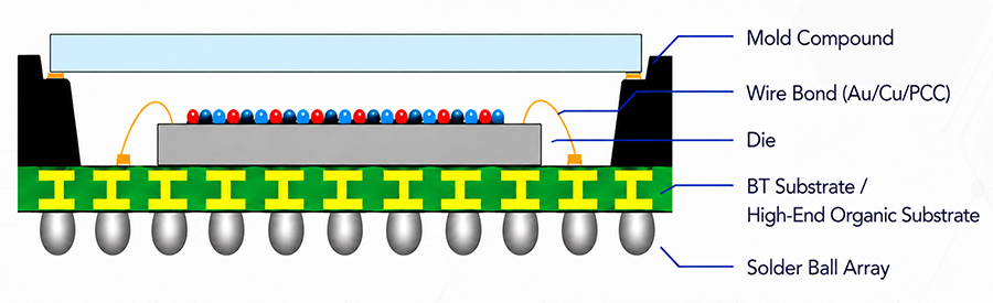
1Fine-Pitch Substrate
•Multi-layer BT substrate
•Fine line/space & microvia
•High routing density in compact size
mPBGA delivers high I/O count, excellent electrical performance,and cost-efficiency in a compact, thin profile for next-generation devices.

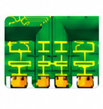
•Multi-layer BT substrate
•Fine line/space & microvia
•High routing density in compact size
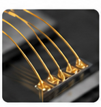
• Ultra-fine Au or Cu/PCC wire
• Low wire loop for thin profile
• Low-stress EMC molding for void-free encapsulation
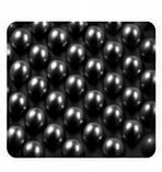
• 0.5mm ~ 0.8mm pitch
• Smaller ball diameter
• Significant X-Y size reduction
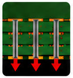
• Power/Ground planes for low parasitics & high SI
• Thermal vias & solder balls for efficient heat dissipation