FCCSP PACKAGE SOLUTION
Flip Chip, Chip Scale, Compact & Cost-effective
FCCSP (Flip Chip Chip Scale Package) utilizes flip chip technology with solder bump interconnects to achieve high I/O density, excellent electrical performance, and compact form factor.

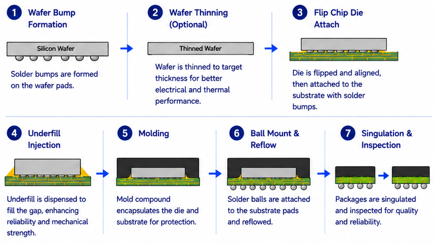
FLIP CHIP PROCESS FLOW
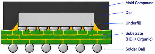
PACKAGE STRUCTURE (CROSS-SECTION)
KEY TECHNOLOGIES
-

Flip Chip Interconnect
Solder bump interconnects provide high I/O density, low inductance, and superior electrical performance.
-

High-Density Substrate
Advanced HDI or organic substrate with fine line/space routing for compact and high-performance design.
-

Underfill Technology
Fills the gap between die and substrate to enhance reliability against thermal cycling and mechanical stress.
-

Fine-Pitch Solder Ball
Small pitch solder balls (e.g., 0.3–0.5mm) enable chip scale package with excellent signal integrity.
-

Mold Protection
Mold compound provides mechanical protection and environmental resistance.